
Microstrip patch antennas are widely used in wireless systems because they are compact, lightweight, inexpensive to manufacture on a PCB, and relatively easy to integrate with RF circuits. In this guide, we will design and simulate a circular microstrip patch antenna for the 2.4 GHz band using ANSYS HFSS. The antenna uses an FR4 dielectric substrate, a copper ground plane, and a microstrip feed. We will also look at the S11 result, explain why a simulated antenna may resonate away from the intended 2.4 GHz frequency, and discuss practical HFSS problems frequently encountered by RF students.
Antenna Design Specifications
The starting parameters for the antenna are:
| Parameter | Value |
|---|---|
| Target frequency | 2.40 GHz |
| Antenna type | Circular microstrip patch |
| Substrate | FR4 |
| Relative permittivity, εr | 4.4 |
| Substrate thickness | 1.60 mm |
| FR4 loss tangent used in model | 0.02 |
| Copper thickness | 0.035 mm |
| Patch radius | 16.95 mm |
| Patch diameter | 33.90 mm |
| 50 Ω feed-line width | ≈3.08 mm |
| Substrate size | 60 mm × 60 mm |
| Ground-plane size | 60 mm × 60 mm |
| Approx. feed length to PCB edge | 13 mm |
| HFSS solution frequency | 2.40 GHz |
| Frequency sweep | 1 GHz to 5 GHz |
Keep in mind that FR4 is not a precision RF dielectric. Its effective dielectric constant and losses can vary between manufacturers and PCB constructions, so εr = 4.4 and tanδ = 0.02 should be treated as the values defined for this simulation rather than universal properties of every FR4 board.
Calculating the Circular Patch Radius
For a circular microstrip patch, the required radius depends mainly on:
- Desired resonant frequency
- Relative permittivity of the substrate
- Substrate thickness
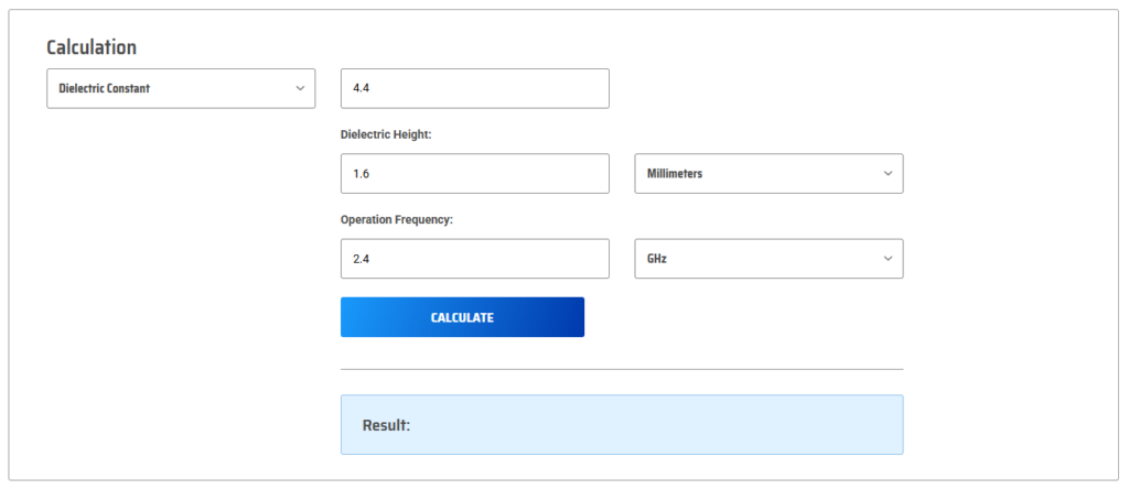
A commonly used circular-patch approximation begins with:
F = 8.791 × 10⁹ / (fr √εr)
and then compensates for fringing fields to obtain the physical patch radius.
For:
- fr = 2.4 GHz
- εr = 4.4
- h = 1.6 mm
the calculated patch radius is approximately:
a ≈ 16.95 mm
Therefore, the circular copper patch has a diameter of approximately:
D ≈ 33.90 mm
This is an excellent starting point, but HFSS optimization is still required because the feed structure, finite ground plane, dielectric model, copper thickness, and fringing fields all influence the final resonant frequency.
Step 1: Create a New HFSS Project
Open ANSYS Electronics Desktop and create a new HFSS design.
For a conventional microstrip antenna, a Driven Modal solution is suitable for many educational designs, particularly when a microstrip line is being excited from the edge of the substrate.
Before drawing the geometry, create variables for important dimensions such as:
freq = 2.4GHzh = 1.6mmpatch_r = 16.95mmfeed_w = 3.08mmsub_w = 60mmsub_l = 60mm
Using variables makes later optimization much easier.
Step 2: Create the Ground Plane
Draw a rectangular sheet on the bottom surface of the antenna.
For the reference design:
Ground plane = 60 mm × 60 mm
Step 3: Create the FR4 Substrate
Create a rectangular box directly above the ground plane.
Use:
60 mm × 60 mm × 1.6 mm
Assign FR4 as its material.
For this simulation:
- Relative permittivity = 4.4
- Loss tangent = 0.02
The dielectric definition is particularly important. An incorrect dielectric constant can noticeably move the resonance frequency.
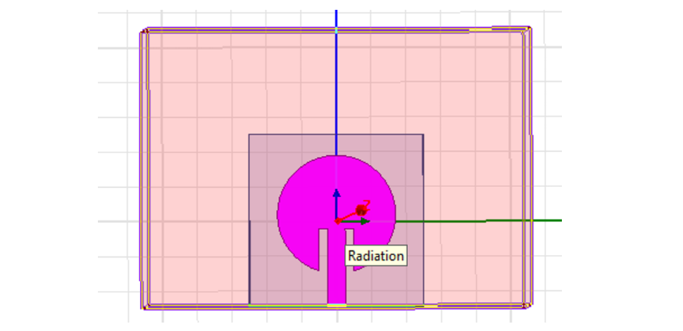
Step 4: Draw the Circular Patch
Create a circular copper sheet on the top surface of the FR4 substrate.
Set:
Radius = 16.95 mm
The patch should remain electrically isolated from the ground by the FR4 dielectric.
The circular patch is the primary resonant structure. Its radius is therefore one of the most effective parameters to tune if the antenna resonates at the wrong frequency.
As a general trend:
- Increasing patch radius lowers the resonant frequency.
- Decreasing patch radius raises the resonant frequency.
Step 5: Add the Microstrip Feed
A microstrip feed can be created from the PCB edge toward the circular patch. For a 1.6 mm FR4 substrate with εr around 4.4, a useful calculated starting width for approximately 50 Ω characteristic impedance is 3.08 mm.
The feed can be connected directly or moved inward using an inset arrangement to improve impedance matching. Do not assume that achieving the correct resonant frequency automatically provides a 50 Ω match. The patch can resonate correctly while still showing poor S11 if the feed location is unsuitable.
Step 6: Create the Air Region and Radiation Boundary
An antenna must radiate into open space, so the antenna should be enclosed inside an air region.
At 2.4 GHz, the free-space wavelength is approximately:
λ₀ ≈ 124.9 mm
One-quarter wavelength is therefore approximately:
λ₀/4 ≈ 31.2 mm
For a conventional HFSS radiation boundary, keeping the boundary approximately one-quarter wavelength away from major radiating structures is a good starting rule. Ansys specifically recommends approximately λ/4 spacing for a standard radiation boundary, although PML boundaries can often be positioned differently.
Assign Radiation to the external faces of the air box.
Step 7: Define the Excitation Port
For a microstrip-fed patch, place the excitation at the feed-line end. A wave port can be used at the substrate edge, with its cross-section including the microstrip conductor, dielectric, and ground reference.
Whichever method you choose, make sure:
- The signal conductor is correctly identified.
- The ground reference is included.
- The port is physically connected to the feed.
- The integration line points from the signal conductor toward ground.
Incorrect excitation is one of the most common reasons an otherwise reasonable patch model produces meaningless S11 results.
Step 8: Configure the HFSS Solution
Create an analysis setup with:
Solution frequency = 2.4 GHz
Then create a frequency sweep.
For our project, a useful broad examination range is:
1 GHz to 5 GHz
For final optimization, however, a narrower sweep around approximately 2.2–2.7 GHz can save simulation time and give better detail around the intended resonance.
Use adaptive meshing and pay particular attention to:
- Feed-to-patch transition
- Inset or narrow gaps
- Patch perimeter
- Port region
The fields change rapidly in these locations, so poor mesh resolution can affect the simulated impedance.
Understanding the S11 Result
An S11 of −16 dB corresponds to a reflection coefficient magnitude of approximately 0.158, meaning only about 2.5% of the incident power is reflected at that particular frequency.
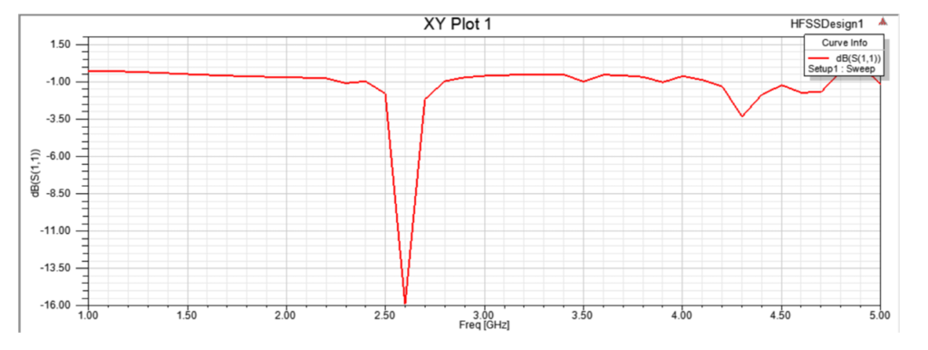
However, the intended design frequency is 2.4 GHz. To move it downward toward 2.4 GHz, try increasing the patch radius slightly and run a parametric sweep.
For example, test values around:
- 16.0 mm
- 16.5 mm
- 16.95 mm
- 17.25 mm
- 17.5 mm
Then observe how the S11 minimum moves.
After locating the resonance near 2.4 GHz, optimize the feed position or inset depth to obtain better impedance matching.
What Results Should You Analyze?
Do not judge an antenna from S11 alone.
A complete HFSS antenna study should examine:
- S11/return loss: Shows impedance matching.
- VSWR: Another representation of mismatch.
- Realized gain: Includes mismatch and antenna losses.
- Directivity: Describes concentration of radiated energy.
- Radiation efficiency: Indicates how much accepted power is radiated rather than dissipated.
- Radiation pattern: Shows where the antenna sends RF energy.
- Surface-current distribution: Helps identify the resonant mode and unwanted modes.
- Smith chart: Useful for determining whether the antenna input is inductive, capacitive, or well matched.
How to Improve the Design
If the antenna does not meet the desired performance, optimize one parameter at a time.
A useful order is:
- Tune the patch radius until resonance reaches the intended frequency.
- Tune the feed/inset location for impedance matching.
- Check the ground and substrate dimensions.
- Verify the FR4 dielectric properties.
- Refine the mesh around the feed and patch edges.
- Recheck the air-box and radiation boundary.
- Finally evaluate gain, efficiency and radiation pattern.
This approach is much more informative than changing several dimensions simultaneously.
Frequently Asked Questions
Why does my 2.4 GHz patch antenna resonate at 2.6 GHz in HFSS?
Usually because the antenna’s effective electrical length is too short. Increase the patch radius slightly. Also verify substrate εr, thickness, feed geometry and boundary setup. Incorrect dielectric properties are a particularly common source of frequency errors. Similar resonance-shift problems are frequently raised by RF designers when simulation and intended frequency do not agree.
Why is my S11 poor even though the patch dimensions are correct?
Resonance and impedance matching are separate problems. The patch may resonate at 2.4 GHz while its input impedance is far from 50 Ω. Adjusting the feed location or using an inset feed can dramatically improve the match. A practical DIY 2.4 GHz patch discussed on Reddit improved significantly after the feed point was effectively moved using an inset structure.
Why do I see more than one dip in my S11 plot?
Not every dip represents the desired fundamental patch mode. Additional minima can result from higher-order patch modes, substrate modes, the feed structure, or other resonant dimensions. Inspect surface-current distributions at each resonance rather than assuming every S11 dip is useful.
Is FR4 suitable for a 2.4 GHz antenna?
Yes, especially for educational and cost-sensitive PCB antennas, but it has higher dielectric loss and greater material variation than dedicated RF laminates. That can reduce efficiency and make fabricated resonance less predictable. Recent RF discussions also show users obtaining reasonable matching on FR4 while still experiencing comparatively modest radiation efficiency.
Should I use a lumped port or a wave port in HFSS?
Either can work when defined correctly. A wave port is convenient when the complete microstrip cross-section ends at a simulation boundary. A lumped port is useful for simpler internal excitation. If the final product uses an SMA connector and connector effects matter, model the launch/connector rather than assuming the ideal port represents the complete physical transition. Port definition is a recurring source of confusion in HFSS projects.
How large should the HFSS air box be?
For a standard radiation boundary, start with approximately λ/4 clearance from the major radiating structure. At 2.4 GHz this is around 31.2 mm in free space. HFSS’s official documentation gives the same quarter-wavelength general recommendation for conventional radiation boundaries.
Why does the fabricated PCB not exactly match the HFSS simulation?
Real boards include dielectric-tolerance variation, copper thickness, manufacturing tolerances, connector parasitics, solder, solder mask and dimensional errors that may be absent from an ideal simulation. Even the dielectric constant of FR4 can vary enough to move a narrow antenna resonance. This is why a final antenna should ideally be measured using a VNA and the measured result compared with simulation.
For complete project documentation, HFSS implementation guidance, antenna design details, simulation support, and related source files, you can contact the Kuwait Academic team through our Contact page.
