
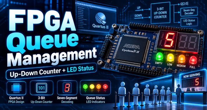
Managing a queue may look simple, but building a digital circuit that counts people entering and leaving requires several important electronics concepts to work together. An FPGA-based queue management system provides a practical way to learn those concepts using an up-down counter, combinational logic and LED indicators.
In this guide, you will learn how to design a basic queue monitoring circuit in Quartus II, verify it with timing simulations and understand how the same design could be expanded for larger queues. We will also cover seven-segment decoding, FPGA pin assignments and common mistakes.
What Is an FPGA-Based Queue Management System?
An FPGA (field-programmable gate array) is a programmable device that can implement digital circuits in hardware. An FPGA implements interconnected logic functions that respond directly to input signals.
A basic queue management system uses an electronic counter to represent how many customers are currently waiting. When a customer joins the queue, an Up control signal increases the stored count. When someone leaves, a Down signal decreases it. The count is then interpreted by a separate decoder, which selects a visual status indicator.
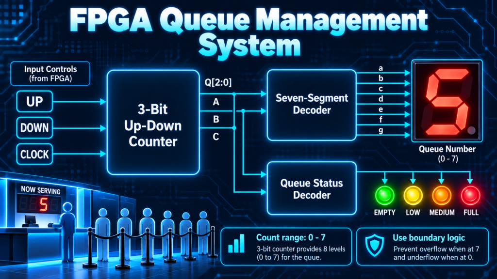
The design discussed here combines a 3-bit up-down counter with four status LEDs: green, yellow, orange and red. Each LED represents a chosen queue occupancy range. The designer must define the count thresholds in the decoder.
The project demonstrates sequential logic, which stores the count, and combinational logic, which translates it into a visible output.
Digital Logic Concepts You Need to Understand
Seven-Segment Displays and Binary Decoding
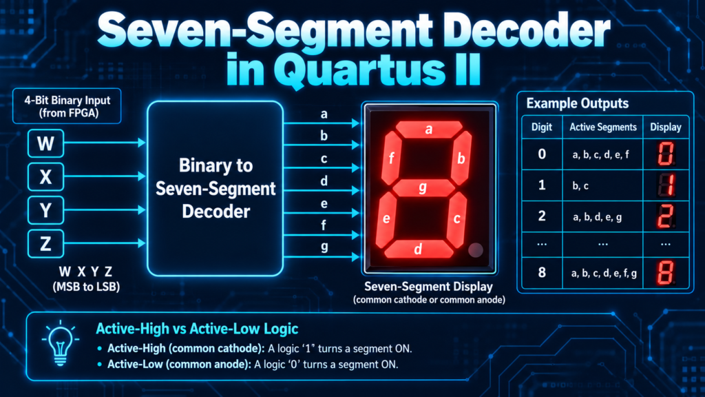
A seven-segment display contains seven individually controlled elements, usually labeled a through g. By switching selected segments on and off, it can show decimal digits. For example, displaying the number 1 normally requires segments b and c, while displaying 8 requires all seven segments.
There are two common display configurations. In a common-cathode display, the shared cathode is connected to the appropriate low potential, and a segment typically turns on when driven high. In a common-anode display, the shared anode connects to the appropriate positive supply, and a segment typically turns on when driven low. Always check the board wiring before choosing output polarity.
A decoder creates the correct seven control signals from a binary input. If a project uses binary-coded decimal (BCD), each decimal digit is represented by four bits. For ordinary decimal decoding, the input values 0000 through 1001 represent digits 0 through 9. Define how the six unused combinations will behave.
Binary Arithmetic and Counters
Binary arithmetic uses the same principles as decimal arithmetic, but each digit has only two possible values: 0 or 1. Half-adders add two input bits, while full-adders also accept a carry input. Larger arithmetic circuits and arithmetic logic units (ALUs) combine these operations to perform useful calculations.
Counters apply binary logic to sequences of events. An up-counter advances through increasing binary values. A down-counter moves in the opposite direction, and an up-down counter supports both directions under control of input signals.
Counters may also be synchronous or asynchronous. In a synchronous design, flip-flops share a clock, making state changes easier to coordinate. In asynchronous or ripple counters, transitions propagate between stages and may introduce additional delays. Timing matters when counter outputs feed an LED decoder.
Tools and Hardware for the FPGA Project
The design can be created with Quartus II, using its schematic editor, Pin Planner and waveform simulation tools. The hardware implementation described here uses a Cyclone IV E FPGA device connected to a seven-segment display.
The queue circuit contains three flip-flops, Up and Down controls, decoding logic and four LED outputs. A clock is necessary to advance the counter. A physical implementation may also need suitable switches or buttons, an appropriate reset arrangement and board-specific I/O configuration.
Before beginning, check the target FPGA board’s pinout, operating voltages and display polarity. Pin numbers vary by board, so assignments should come from its documentation rather than from another design’s screenshot.
How to Design a Seven-Segment Decoder in Quartus II
Step 1: Create the Truth Table
Start with four input signals, labeled W, X, Y and Z, and seven outputs, labeled a, b, c, d, e, f and g. For each input value representing a decimal digit, record which segments should illuminate. The truth table connects the desired visual result to precise digital output conditions.
Be consistent about whether a logical 0 or 1 turns on a segment. This matters for an active-low display, where a 0 turns on a segment.
Step 2: Simplify the Boolean Logic
Use Karnaugh maps (K-maps) to simplify the expression for each segment output. Simplification can reduce gate count, but depends on the truth table and treatment of unused states.
Create the combinational schematic in Quartus II by connecting the required gates. Check all seven output paths independently instead of assuming that one working digit proves the entire decoder is correct.
Step 3: Assign FPGA Pins and Test the Display
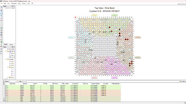
Open Pin Planner and map W, X, Y and Z to the intended FPGA inputs. Then assign a through g to the physical outputs wired to the seven-segment display. Verify the I/O standard and voltage compatibility with the board.
Run a simulation before programming the FPGA. Test several input combinations and confirm the expected segments activate. Incorrect pin mapping, reversed bit order and active-low logic are common reasons a working schematic displays the wrong number on hardware.
Building a 3-Bit Up-Down Counter
Understanding the Counter States
The queue counter stores its value in three bits, identified as A, B and C. Three bits provide 2³ = 8 distinct states, from binary 000 through 111, representing decimal counts 0 through 7.
For example, consecutive increases from zero produce 000, 001, 010, 011 and so on, assuming the bits are interpreted in the intended least-significant-to-most-significant order. Decrementing reverses this progression. Match each output name to its bit significance when wiring the decoder.
An important practical limitation is that a plain three-bit binary counter may wrap around after its maximum or minimum state. A real queue monitor should prevent an arrival from increasing a full count or a departure from creating a negative count. These boundary controls are useful improvements rather than something to assume is already built into every schematic.
Create the Counter Schematic
In Quartus II, construct the sequential counter using three flip-flops and the control logic needed to select upward or downward counting. Connect the clock and label the Up, Down, A, B and C signals clearly. The counter must be designed so that its behavior for both controls being active, or neither being active, is defined.
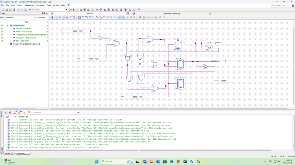
Verify the Counter with a Timing Diagram
Simulation checks whether the circuit changes state at the expected clock edges. For an upward-counting test, set Up = 1 and Down = 0. In the illustrated simulation, the clock signal toggles every 10 ns, and the output signals follow the binary counting sequence.
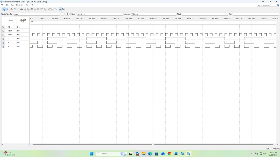
Inspect the waveforms rather than checking only the final count. Check transitions against the clock edge, control state and bit order before integrating the decoder.
Combining the Counter and Queue Status Decoder
The complete FPGA queue management system connects the A, B and C counter outputs to a combinational decoder. That decoder drives green, yellow, orange and red status LEDs, allowing an operator to interpret the queue level without reading the raw binary number.
The counter and decoder have different responsibilities. The counter remembers the current state; the decoder immediately determines which LED output should be active for that state. When designing the decoder, decide exactly which of the eight counts belongs to each status category and make the selection unambiguous.
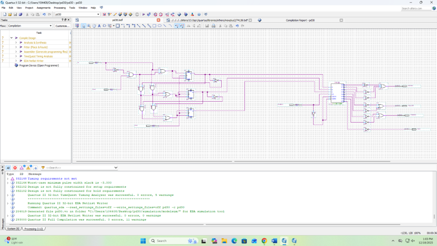
Pay special attention to most significant bit (MSB) and least significant bit (LSB) connections. A reversed connection may not prevent the system from running, but it can cause an LED to indicate the wrong queue condition.
Test 1: Increasing the Queue Count
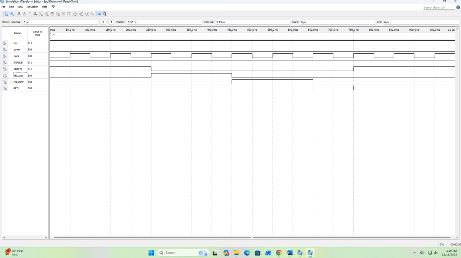
Set Up = 1 and Down = 0, then apply clock transitions. The stored value should increase in binary order, and the LED outputs should respond whenever the count enters another defined status range.
Test 2: Decreasing the Queue Count
Next, set Up = 0 and Down = 1. The counter should move through decreasing values, and the status decoder should update accordingly. Test transitions around each status boundary as well as ordinary intermediate states.
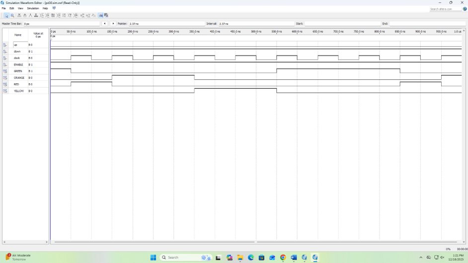
Simulations verify the tested inputs, but cannot replace real-board testing.
Common FPGA Design Problems and How to Fix Them
Seven-Segment Display Shows Incorrect Digits
Check whether the display uses active-high or active-low signaling. Review your truth table, Boolean expressions and physical pin assignments. Also confirm that the selected binary input order matches the display decoder’s expectations.
Counter Outputs Change Unexpectedly
Check clock connections, flip-flop inputs and control signal definitions. Inspect the simulation around the exact clock edge. If physical push buttons are used, contact bounce can produce multiple unintended transitions; a debouncing circuit can help.
LED Status Does Not Match the Queue Count
Review the decoder’s selected ranges and confirm that A, B and C are connected in the correct bit order. Test all eight possible counter states rather than checking only the first and last values.
Simulation Works but FPGA Hardware Does Not
Revisit Pin Planner assignments, voltage standards, clock selection and board connections. Confirm that the schematic has been compiled for the correct FPGA device and that the configuration was uploaded successfully.
How to Expand the Design to 40 Customers
A three-bit counter cannot represent a queue of 40 people. To represent counts from 0 to 40 inclusive, the design requires at least six bits, because five bits represent only 32 states, while six bits represent 64 states.
A six-bit counter alone is not sufficient for a reliable 40-person limit: it can count beyond 40 unless extra logic blocks further increments. The expanded system should also prevent counts below zero, revise the decoder thresholds and provide a clearer numeric display when needed.
For future development, consider implementing the circuit in Verilog or VHDL rather than relying entirely on schematic entry. Other useful upgrades include a seven-segment queue number display, push-button input, button debouncing and a dedicated reset function. These changes can make the design easier to operate, maintain and scale.
Frequently Asked Questions
What is the purpose of an FPGA queue management system?
Its purpose is to count arrivals and departures using digital hardware and indicate the queue’s occupancy level through outputs such as colored LEDs. It also provides a useful example of integrating counters and decoder logic.
Why is a 3-bit counter used in this project?
Three bits are sufficient for eight binary states, representing counts 0 to 7. This small state space makes the design straightforward to simulate, inspect and connect to a status decoder.
What is the difference between a counter and a decoder?
A counter is a sequential circuit that stores a state and changes it in response to control inputs and clock events. A decoder is a combinational circuit that interprets an input pattern and generates the required output signals.
Can Quartus II simulate the circuit before FPGA programming?
Yes. Waveform-based simulation can verify the intended relationships among the clock, Up and Down controls, counter bits and LED outputs. Physical board testing is still needed to check pin wiring and real input behavior.
Why is active-low logic important for seven-segment displays?
On an active-low connection, a low output turns on a segment. If the Boolean logic assumes high means on, the resulting digit can be incorrect. The FPGA board’s actual display wiring determines the required signal polarity.
How many bits are needed for a 40-customer queue?
At least six bits are needed to represent every value from 0 through 40. Additional boundary logic should prevent counts above 40 and below zero.
Conclusion
An FPGA-based queue management system is an accessible way to combine digital theory with practical circuit design. The seven-segment decoder introduces truth tables, Boolean simplification and pin mapping; the three-bit counter demonstrates sequential behavior; and the four-LED queue indicator shows how both types of logic operate together.
By building the schematic in Quartus II, checking the timing diagrams and then validating the hardware, students can develop a stronger understanding of digital design. The same foundation can support larger counters, numeric displays and more capable queue monitoring systems.
For more information, please feel free to reach out to us through our Contact page.
